You must be very creative today to effectively match the shielding solution to the size of the components and circuits on the PCB.
Today's RF engineers are faced with new challenges when designing wireless communications devices. Modern cell phones have incorporated many features such as cameras, large multimedia displays, and multifrequency and multimode operation in smaller form factors than previously were available.
Even in the GPS and satellite radio markets devices are smaller and more integrated. For instance, miniature antenna technologies from companies like Sarantel Plc accommodate compact portable, Bluetooth -enabled GPS receivers.
This trend has driven RF engineers to require that PCBs have integrated shielding at the board level. This ensures that the circuit is fully operational and compliant as a stand-alone component of the wireless device.
Traditionally, PCB manufacturers have used stamped metal or drawn metal cans, soldered to the PCB during the manufacturing reflow process, to shield sensitive RF components. These solid metal cans usually feature an array of perforated holes to aid in the heat transfer to the components under the can during the reflow process (Figure 1a).
These types of shields do not easily allow for rework or inspection after the can has been soldered to the PCB. Because of this, variations of soldered cans with removable lids have emerged over the years (Figure 1b and Figure 1c).
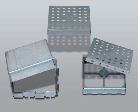
These products have an outer fence or frame that is soldered to the PCB during the reflow process and a separate lid that attaches to this frame using either a knife-edge contact or interference fit between the lid and can. These removable-lid cans provide easy access to the components for rework or inspection.
Some products made from metalized plastic materials attach to the PCB using adhesive technology. However, special tools are required to remove the adhesive-type shield from the PCB should it need to be replaced.
The XGR Snapshot technology is a PCB-level approach that provides a lightweight, easily removable shield (Figure 2). Because this shield is thermoformed, designers can lay out the shield enclosure to fit their circuits rather than constraining their circuit layout to the rectangular dimensions of a can. This feature allows for complex geometries in a very compact, multicavity, one-piece shield.
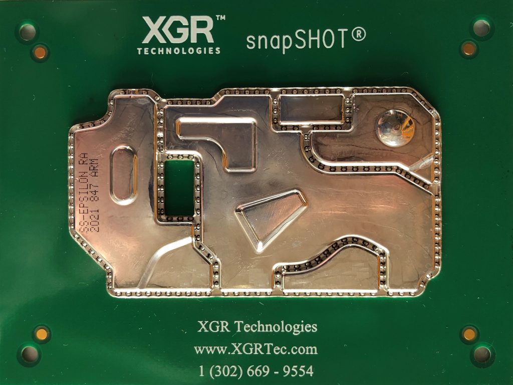
The BGA ball attachment method provides the mechanical connection to the PCB as well as electrical contact for shielding. The shield is flexible and conforms to the PCB surface. The metallization for the shield is applied to the outside of the can, so there is little concern about the can shorting out to components underneath. If you want to rework or inspect a component under the shield, the existing shield is pulled off and another shield snapped on after the work is finished.
PCB-level shields are designed to protect certain RF portions from other sections of the circuit, such as transmit from receive, as well as from outside interference. To determine the effectiveness of a shield, you must derive a test method that closely represents the environment that typical surface-mount (SM) components exist in.
Much work has been done to develop a PCB-level test method for EMI shields. Figure 3 shows a test PCB with a snapSHOT shield. Figure 3a displays two radiating devices about one inch apart, one under the shield that represents the susceptible RF components and one next to the shield representing the aggressor.
In this manner, the shielding effectiveness (SE) of the enclosure can be measured as if a component next to the shield were potentially coupling to the circuit inside. Custom SMA connectors, designed to make a complete solder connection to the ground plane, attach the test equipment to the radiators on the test PCB (Figure 3b).
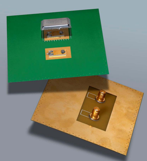
Using the test fixture, a far-field test can be performed by making measurements in a mode-stirred reverberation chamber, which uses a horn antenna connected to an RF source to illuminate the inside of the room with radiated energy. The device under the shield then becomes the receiver, and when connected to a spectrum analyzer, coupled power can be measured. The SE can be determined by comparing the results with and without the shield attached.
An important factor to consider when using shielded enclosures is the resonant frequency of the cavity inside the box. Because energy is stored inside the cavity at these resonant frequencies, the SE can be significantly compromised. Knowing this helps to explain the resonant behavior of the data and provides a guideline to RF engineers when specifying shielded enclosure dimensions.
Equation 1 shows the calculation for the resonant frequency conditions. The actual resonant frequency of the box most likely will be slightly lower due to dielectric materials inside the volume and apertures through the walls that make the dimensions of the cavity electrically larger.
A simple test fixture can be used to measure the resonant frequencies of PCB-level shields.1,2,3,4 The test fixture demonstrates the coupling between two components about 0.5 inches apart and how a shielded enclosure affects this coupling.
As an example, the curves in Figure 4a show the coupling with and without the metal can shown in Figure 1a (which is about 1 inch square and 0.2 inches tall). The blue trace displays very little coupling without any shield in place, and the red trace shows the increased coupling due to the shield. The first resonant frequency is shown to be about 7.7 GHz, and the next is 12.5 GHz.
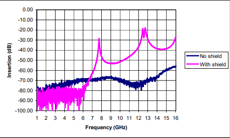
If the formula is used to calculate the theoretical frequencies, the first TE011 mode will be 8.2 GHz, and the second and third, TE012and TE021 modes, will be 13 GHz. These second and third frequencies are called degenerate modes and shown slightly separated in Figure 4a.
Again, the actual frequencies are slightly lower than the theoretical due to dielectric materials and apertures. This exercise is important because it helps to explain certain resonant conditions in the SE data and aid the RF engineer in selecting properly sized shields.
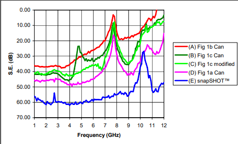
The SE curves for the cans in Figure 1 and the snapSHOT shield in Figure 3 are shown in Figure 4b. This data was collected using the test PCB with a radiator inside and outside of the shield. A medium power source was used to drive the outside radiator, and a phase-locked spectrum analyzer was used to receive the signal from the inside radiator.
The SE is computed by taking the difference of the received power with and without the shield. A positive SE implies attenuation when the shield is applied.
Figures 4a and 4b show varying levels of SE with several resonant peaks. The three cans tested had the same overall dimensions so they exhibit the same basic resonant frequency structure.
With all of the cans, the SE is substantially decreased at the predicated resonant frequency of 7.7 GHz. The snapSHOT shield had smaller overall dimensions so its first resonant peak occurred at 10.3 GHz. This artifact is to be expected with most PCB-level shields at the resonant frequencies of the cavity.
Most RF engineers would try to design the cavity so that the maximum operating frequency was well below the first resonant frequency of the enclosure. The flatness of the SE data at the lower frequencies can be explained by the fact that apertures in the shield walls, the attachment points to the ground trace, and the vias that connect the ground trace to the ground plane are all in the near field of the radiators. Further explanation of this phenomenon is available in the references, particularly reference 4.
Of the three cans, the perforated solid metal can (trace D) shows the best SE (about 45 dB) in an operating frequency range up to about 6 GHz. This can does not have a removable lid but was included to provide a point of reference.
The least amount of shielding was shown by the can in Figure 1b, displayed as trace A, which is in the mid 30-dB range. This particular can has the largest apertures, which causes the greatest opportunity for EMI leakage.
The can in Figure 1c, a removable-lid version of the can in Figure 1a, had a nominal shielding in the low 40-dB range, with an unexpected resonance at about 4.8 GHz. This resonance is below the first resonance of the cavity because it has a justify bridged section required for pick-and-place vacuum SM technology (SMT) (Figure 1c). If this bridge does not make intimate contact to the lid, it may resonate.
This data was confirmed on several samples of varying sizes. A further demonstration of this is shown in trace C where the bridge was cut out of the sample from trace B and remeasured. You can see that the 4.8-GHz resonance is no longer present.
The snapSHOT data, displayed as trace E, shows SE of about 60 dB. This is almost a 20-dB improvement over the removable lid cans that were tested in this experiment.
A far-field SE test performed inside a mode-stirred reverberation chamber on each of the samples with and without the shield correlated within a few decibels of the data shown in Figure 4b.
Conclusion: Next-generation wireless devices are requiring more challenging electronic packaging techniques that, in turn, directly influence EMI shielding solutions. RF engineers need to be able to apply complex geometries to their circuits and PCB layouts to achieve smaller and more integrated circuits.
As a result, engineers must be very creative when matching the shielding solution to the size of the components and circuits on the PCB. If rework or inspection is a requirement, then one solution is a removable shield that is easily pulled off and replaced with another when the work is complete.
Reference: www.electronicdesign.com


