PCB (Printed Circuit Board) design is at the heart of modern electronics. It's the intricate process of transforming ideas into functional circuitry that powers our devices. In this comprehensive guide, we'll take you on a journey through the world of PCB design, from the initial concept to the creation of a fully functional board.
Table of Contents
- Chapter 1: PCB Design Basics
- Chapter 2: The PCB Design Process
- Chapter 3: Choosing the Right PCB Design Software
- Chapter 4: Component Selection and Placement
- Chapter 5: PCB Layer Stackup and Materials
- Chapter 6: Traces and Routing Guidelines
- Chapter 7: Grounding and Power Planes
- Chapter 8: Signal Integrity and EMI/EMC
- Chapter 9: Thermal Management
- Chapter 10: Design for Manufacturability (DFM)
- Chapter 11: Design Validation and Simulation
- Chapter 12: Design for Testability (DFT)
- Chapter 13: Documentation and Collaboration
- Chapter 14: Regulatory Compliance
- Chapter 15: PCB Prototyping and Iteration
- Conclusion: Mastering PCB Design
Chapter 1: PCB Design Basics

In the vast landscape of modern electronics, Printed Circuit Boards (PCBs) are the unsung heroes that make it all possible. These intricate and often compact boards serve as the foundation for electronic devices, connecting and controlling the flow of electrical signals. In this chapter, we will embark on a journey through the fundamentals of PCB design, shedding light on their significance and the core components that bring them to life.
1.1 Introduction to PCBs
PCBs, short for Printed Circuit Boards, are the backbone of electronic devices. They provide a platform for connecting various electronic components, allowing them to communicate and work together seamlessly.
The evolution of PCBs has revolutionized electronics, enabling the creation of compact, reliable, and complex devices that have become an integral part of our daily lives.
1.2 The Significance of PCBs in Electronics
PCBs act as the central nervous system of electronic devices, facilitating the flow of electricity and data between components.
Their design and layout significantly impact the performance, reliability, and functionality of electronic devices.
PCBs play a crucial role in miniaturizing electronic products, making them smaller, lighter, and more portable.
1.3 Key Components of a PCB
Substrate: The substrate is the base material of the PCB, typically made of fiberglass-reinforced epoxy resin (FR-4). It provides mechanical support and electrical insulation.
Copper Layers: Copper layers, known as traces, form the conductive pathways on the PCB. They carry electrical signals and connect various components.
Pads: Pads are small metal areas on the PCB's surface where electronic components are soldered or attached.
Vias: Vias are small holes filled with metal that connect traces on different layers of the PCB, enabling the flow of signals between layers.
Components: Electronic components, such as resistors, capacitors, integrated circuits (ICs), and connectors, are mounted on the PCB. They perform specific functions within the circuit.
Solder Mask: A solder mask is a protective layer applied to the PCB's surface, leaving only the pads exposed for soldering. It prevents unintended electrical connections and oxidation.
Silkscreen: The silkscreen layer includes text, symbols, and markings on the PCB's surface, aiding in component placement and identification.
In this chapter, we've laid the foundation for our journey into the world of PCB design. Understanding the basics of PCBs and their critical role in electronics is the first step towards mastering the art and science of PCB design.
Chapter 2: The PCB Design Process
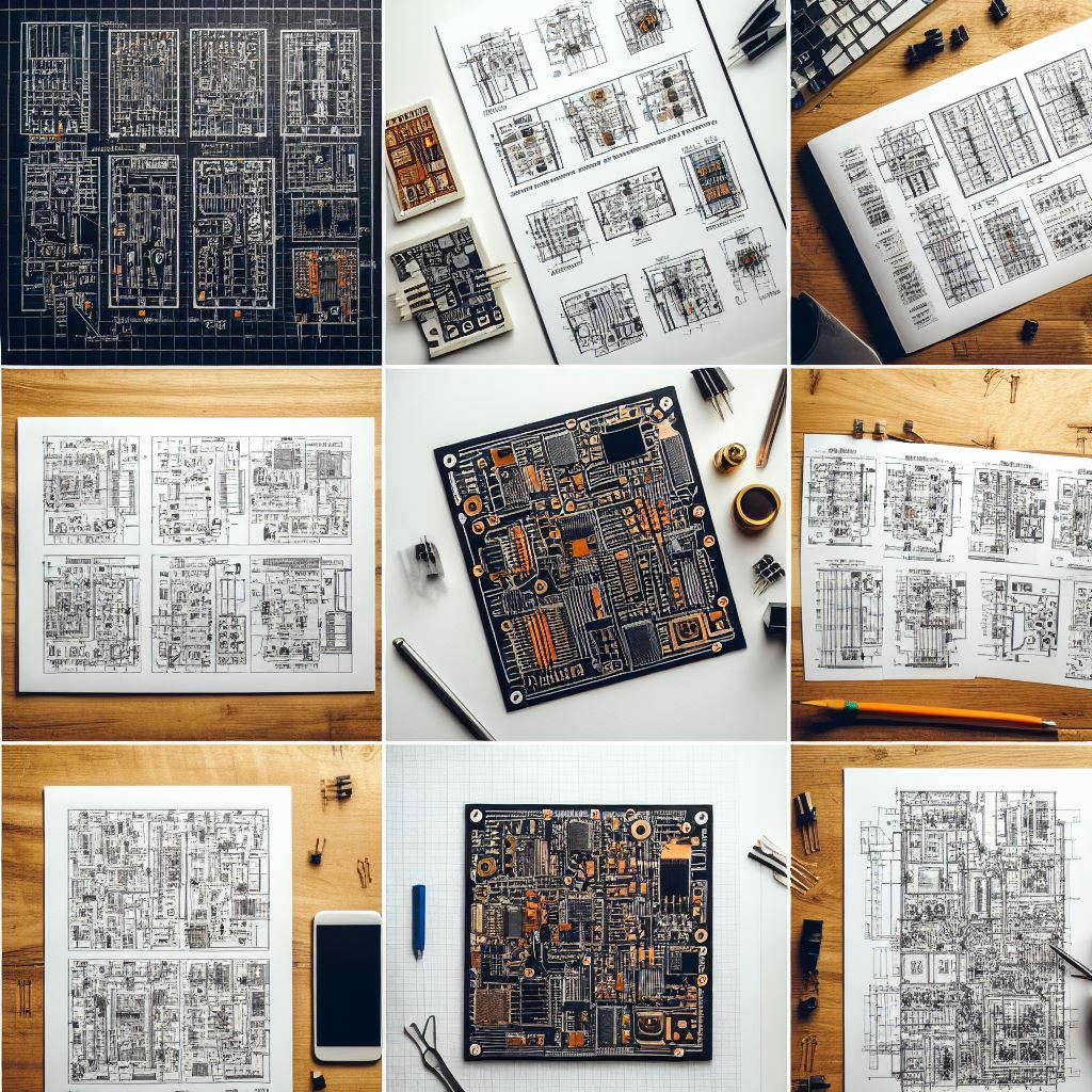
Once you grasp the basics of PCBs and their significance, it's time to embark on the journey of PCB design. This chapter provides a comprehensive breakdown of the PCB design process, from conceptualization to the creation of a functional and reliable board. We'll explore each step and delve into how to define design requirements and constraints effectively.
2.1 Conceptualization and Requirements Gathering
Project Initiation: The PCB design process begins with defining the project scope, objectives, and goals. Identify the purpose of the PCB, the intended application, and key performance requirements.
Requirements Gathering: Work closely with stakeholders to gather detailed requirements. Consider factors such as electrical specifications, form factor, environmental conditions, and budget constraints.
2.2 Schematic Design
Schematic Capture: Create an electronic schematic diagram that represents the electrical connections between components. Use specialized software tools for schematic design.
Component Selection: Choose electronic components based on the project's requirements. Consider factors like component availability, cost, and functionality.
2.3 Component Placement and Routing
Component Placement: Position components on the PCB layout for optimal electrical performance and efficient use of space. Consider signal integrity, thermal management, and ease of assembly.
Routing: Connect components using traces, ensuring proper signal paths and avoiding cross-talk. Observe design rules, such as trace width, spacing, and clearance.
2.4 Layer Stackup and PCB Materials
Layer Stackup: Determine the number of layers in the PCB and their arrangement. Consider multilayer designs for complex circuits.
Material Selection: Choose appropriate materials, such as substrate and copper thickness, based on the application's thermal and electrical requirements.
2.5 Design Validation and Simulation
Design Validation: Perform simulations and analyses to verify the design's functionality, signal integrity, and thermal performance.
Iterative Refinement: Address any issues identified during validation, making necessary design adjustments.
2.6 Design Documentation
Creation of Design Files: Generate comprehensive design files, including Gerber files, Bill of Materials (BOM), assembly drawings, and manufacturing notes.
Collaboration: Share design documentation with team members, fabricators, and assemblers for smooth production.
2.7 Design for Manufacturability (DFM)
DFM Considerations: Optimize the design for ease of manufacturing and assembly. Minimize complexity and ensure components are readily available.
2.8 Regulatory Compliance
Standards and Certification: Ensure the design complies with industry-specific standards and regulations. Plan for certification and testing.
2.9 Prototyping and Testing
Prototyping: Create a prototype of the PCB to validate its performance in a real-world environment.
Testing: Conduct thorough testing and debugging to identify and resolve any issues.
2.10 Finalization and Production
Final Design Approval: Obtain final approval from stakeholders and prepare for production.
Production: Hand off design files to PCB manufacturers and assemblers for mass production.
This chapter provides a roadmap for the PCB design process, highlighting each step's significance and interplay. Effective design requirements and constraints definition at the outset are crucial for guiding the design process toward a successful outcome.
Chapter 3: Choosing the Right PCB Design Software
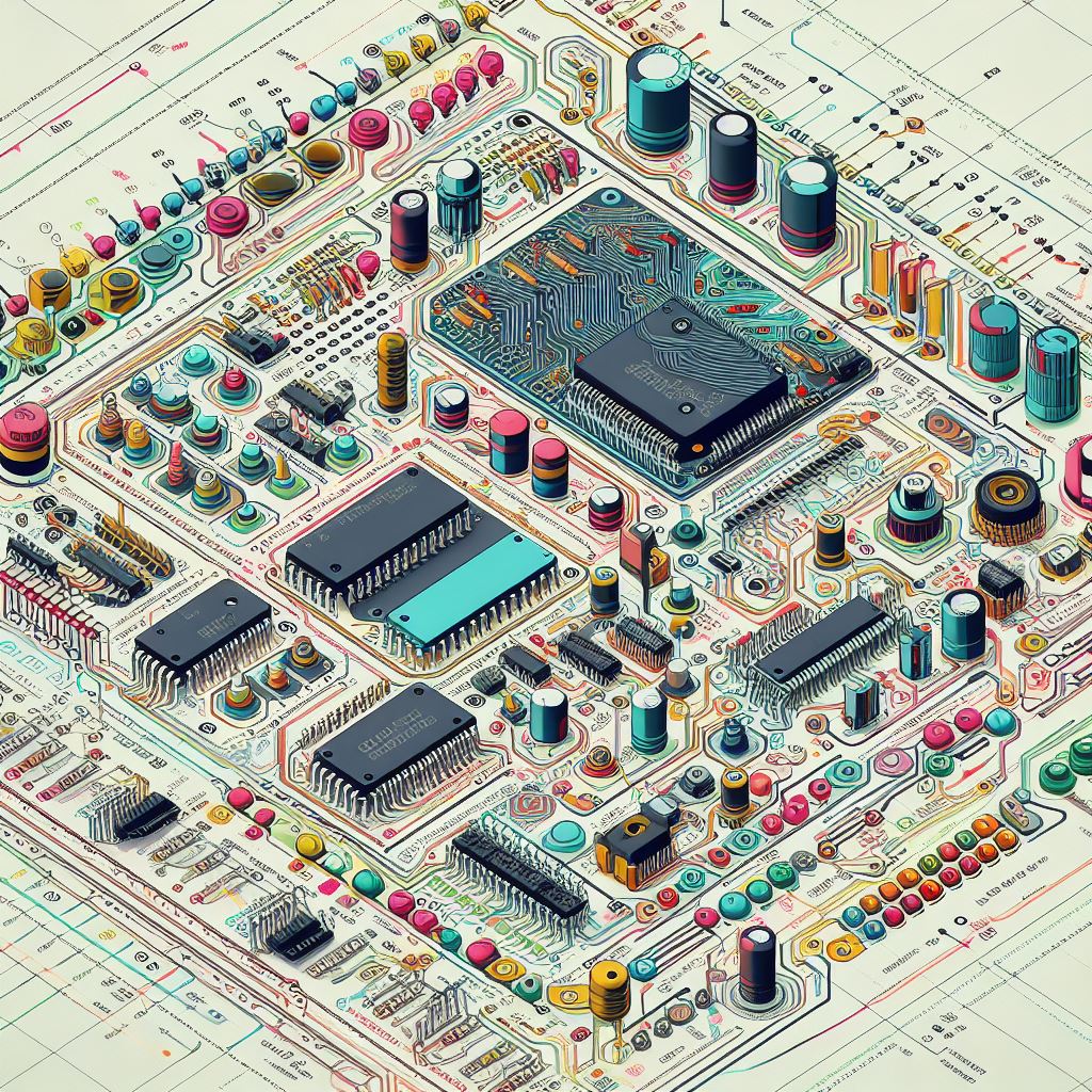
Selecting the right PCB design software is a pivotal decision in the PCB design process. In this chapter, we'll provide you with an overview of some of the popular PCB design software tools available and offer tips to help you make an informed choice that aligns with your project's needs.
3.1 The Significance of PCB Design Software
PCB design software serves as the digital canvas where your PCB design takes shape. It empowers designers to create schematics, lay out components, and route traces with precision.
The choice of software impacts your design efficiency, collaboration capabilities, and the quality of the final product.
3.2 Popular PCB Design Software Tools
There is a diverse range of PCB design software tools available, catering to various design requirements and user preferences. Some of the most widely used software tools include:
- Altium Designer: Known for its user-friendly interface and powerful capabilities, Altium Designer is a favourite among professional PCB designers. It offers features for schematic capture, component placement, and real-time collaboration.
- Eagle: Eagle, by Autodesk, is renowned for its accessibility and affordability. It's suitable for beginners and hobbyists, offering a vast library of components.
- KiCad: An open-source option, KiCad has gained popularity for its extensive features, making it a cost-effective choice for both beginners and professionals.
- Cadence Allegro: This robust software is favoured for its high-quality routing and integration with other design tools.
- OrCAD: OrCAD offers a comprehensive suite of PCB design tools, including schematic capture, PCB layout, and simulation.
- PADS: PADS by Siemens provides a range of design capabilities and is suitable for small to medium-sized businesses.
3.3 Tips for Selecting PCB Design Software
Choosing the right PCB design software should align with your specific project requirements and expertise level. Here are some tips to consider:
Project Complexity: Assess the complexity of your project. For simple designs, user-friendly and cost-effective software may suffice. Complex projects may require high-end software with advanced features.
Learning Curve: Consider your familiarity with PCB design software. Some tools are more intuitive for beginners, while others may have a steeper learning curve but offer advanced capabilities.
Compatibility: Ensure that the software you choose is compatible with your operating system and can import/export necessary file formats.
Collaboration: If you're working in a team, opt for software that supports real-time collaboration and version control.
Cost: Evaluate the software's pricing structure, including licensing, maintenance, and additional features. Factor in your budget constraints.
Support and Community: Research the availability of support resources, forums, and a user community to assist you when you encounter challenges.
Future Scalability: Consider whether the software can accommodate future project expansions and evolving design requirements.
Integration: If you use other design tools or software, ensure compatibility and integration capabilities.
Trial Period: Many software providers offer trial periods. Take advantage of these to test the software's suitability for your project.
Choosing the right PCB design software is a critical step in ensuring the success of your PCB design project. By assessing your project's specific needs, your level of expertise, and your budget, you can make an informed choice that empowers you to bring your PCB design ideas to life efficiently and effectively.
Chapter 4: Component Selection and Placement

The heart of any PCB design lies in its components. Selecting the right components and placing them strategically on the board is a pivotal step towards creating a functional and efficient PCB. In this chapter, we'll explore guidelines for selecting components based on specifications and strategies for their efficient placement.
4.1 Component Selection Guidelines
Understanding Component Specifications: Begin by thoroughly understanding the electrical and mechanical specifications of the components you need. Key parameters include voltage ratings, current ratings, package sizes, and temperature tolerances.
Component Availability: Consider component availability and lead times. Ensure that the chosen components are readily accessible from suppliers to prevent delays in your project.
Cost vs. Performance: Strive for a balance between component cost and performance. While it's essential to manage expenses, compromising on component quality can lead to reliability issues.
Environmental Considerations: If your PCB will operate in challenging environments, such as extreme temperatures or high humidity, select components that can withstand these conditions.
Compatibility: Ensure that components are compatible with your chosen PCB design software and footprint libraries.
Longevity: Evaluate the long-term availability of components, especially if your project requires long production cycles.
4.2 Component Placement Strategies
Efficient component placement significantly influences PCB performance, reliability, and manufacturability. Here are some strategies to optimize this crucial phase:
Functional Grouping: Group components based on their functions or subsystems. This makes it easier to route traces and minimizes signal interference.
Signal Flow: Arrange components in a way that follows the logical flow of signals. For example, start with the power supply components and follow the signal path from input to output.
Component Orientation: Align components uniformly, either horizontally or vertically, to improve the PCB's aesthetic appeal and ease of assembly.
High-Speed Signals: Place critical high-speed components closer to each other to reduce signal trace lengths and minimize signal loss.
Thermal Considerations: Components that generate heat should be placed strategically to optimize thermal dissipation. Consider airflow and thermal vias if necessary.
Keep-Out Areas: Define keep-out areas to prevent components from encroaching on critical zones or interfering with mechanical features.
Test Points: Include test points for easy access during debugging and testing phases.
Manufacturability: Ensure that component placement aligns with the capabilities of your chosen manufacturer, including pick-and-place machines.
Layer Distribution: Distribute components across different PCB layers to minimize signal crosstalk and achieve a balanced design.
Flexibility: Maintain some flexibility in component placement to accommodate changes and optimizations during the design process.
4.3 Simulation and Validation
Before finalizing component placement, consider running simulations and analyses to assess the design's performance. Tools like signal integrity simulators can help identify potential issues with signal quality and interference.
4.4 Design Iteration
Component placement is often an iterative process. Be prepared to make adjustments based on simulation results, manufacturability constraints, and other considerations. Iterative refinement can lead to an optimal layout.
Effective component selection and placement are essential elements of successful PCB design. By adhering to guidelines, considering the PCB's specific requirements, and employing thoughtful placement strategies, you can create a well-organized and efficient PCB layout that meets your project's objectives.
Chapter 5: PCB Layer Stackup and Materials
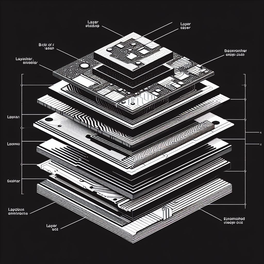
In this chapter, we delve into the foundational aspects of multilayer PCB design: layer stackup and materials selection. These elements are critical to achieving the desired electrical and mechanical performance of your PCB.
5.1 The Significance of Layer Stackup
Multilayer PCBs: While single-layer and double-layer PCBs have their applications, many modern electronics demand the complexity and compactness offered by multilayer PCBs. A multilayer PCB consists of multiple layers of conductive traces and insulating substrate material stacked together.
Signal Integrity: The stackup determines the arrangement of signal, power, and ground planes. A well-designed stackup is essential for preserving signal integrity, reducing electromagnetic interference (EMI), and efficiently routing traces.
Impedance Control: Layer stackup is crucial for controlling impedance in high-speed digital and RF circuits. The arrangement of layers impacts the characteristic impedance of transmission lines.
Thermal Management: For applications with components that generate heat, the stackup can help dissipate heat efficiently, contributing to the PCB's thermal performance.
5.2 Selecting the Right Materials
Substrate Material: The substrate material forms the core of the PCB and affects its electrical, thermal, and mechanical properties. Common materials include FR-4, FR-408, and polyimide. The choice depends on factors like operating conditions, cost, and electrical requirements.
Copper Thickness: The thickness of the copper layers impacts the PCB's current-carrying capacity and thermal conductivity. Copper weights are specified in ounces per square foot (oz/ft² or commonly referred to as copper weight).
Prepregs and Cores: Prepregs are insulating layers between copper layers, while cores are solid, copper-clad layers. These materials contribute to the overall rigidity and electrical properties of the PCB.
Dielectric Constant (Dk): Dk is a critical parameter, especially in high-frequency applications. It influences signal propagation speed and impedance. Matching the Dk of the substrate to the components' requirements is crucial.
Tg (Glass Transition Temperature): Tg is the temperature at which the substrate material transitions from a solid to a soft, rubbery state. It affects the PCB's thermal stability during assembly processes.
5.3 Design Considerations
Layer Count: Determine the number of layers required based on the complexity of your design. Multilayer PCBs provide greater routing flexibility but also increase manufacturing costs.
Symmetry: Achieve symmetry in the layer stackup when possible. This aids in balancing mechanical stress and improving manufacturability.
Power and Ground Planes: Include dedicated power and ground planes for improved signal integrity, reduced EMI, and efficient power distribution.
Signal Layers: Ensure there are enough signal layers for routing traces without excessive crosstalk.
5.4 Manufacturing and Cost Considerations
Stackup Compatibility: Ensure that your chosen stackup is manufactural by your selected PCB manufacturer. Discuss stackup options with your manufacturer to align with their capabilities.
Cost vs. Performance: Balance your design's performance requirements with the available budget. Exotic materials and complex stackups can significantly increase manufacturing costs.
Material Availability: Verify the availability of selected materials to prevent delays in production.
5.5 Layer Stackup Documentation
Document your layer stackup thoroughly in your design files and communicate it clearly with your PCB manufacturer. Include details about materials, layer thicknesses, copper weights, and dielectric properties.
A well-considered layer stackup and material selection process is fundamental to achieving the desired functionality, performance, and reliability of your PCB design.
Chapter 6: Traces and Routing Guidelines
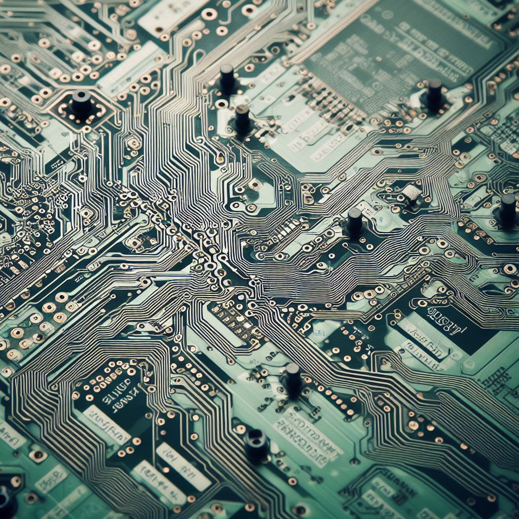
Efficient and precise routing of traces on your PCB is vital for ensuring signal integrity, minimizing interference, and achieving a functional design. In this chapter, we will delve into the critical aspects of trace width, spacing, and routing best practices while highlighting common routing mistakes to avoid.
6.1 Trace Width and Spacing
Trace Width: The width of traces determines their current-carrying capacity. Calculate the required trace width based on the expected current and temperature rise constraints. Ensure that your design adheres to industry standards and manufacturer recommendations.
Spacing: Spacing between traces and between traces and adjacent components is crucial for preventing electrical interference (crosstalk) and ensuring manufacturability. Consider factors such as the dielectric constant of the substrate material and the desired impedance.
6.2 Routing Best Practices
Signal Integrity: Follow the principles of signal integrity to minimize reflections, signal degradation, and electromagnetic interference (EMI). Maintain controlled impedance for high-speed signals by adhering to specific trace widths and spacing.
Short and Direct Paths: Keep traces as short and direct as possible, especially for high-frequency signals. Minimize the use of vias and avoid sharp corners, which can lead to signal distortion.
Power and Ground Planes: Connect power and ground planes with multiple vias to create low-impedance paths for return currents. This reduces noise and enhances signal quality.
Component Placement: Strategic placement of components can simplify routing. Group related components together and place critical components close to each other to minimize trace lengths.
Differential Pairs: Maintain consistent spacing and length for traces in differential pairs to ensure balanced signal propagation and reduce common-mode noise.
Bypass Capacitors: Place bypass capacitors close to the power pins of ICs to minimize voltage fluctuations and ensure stable operation.
6.3 Avoiding Common Routing Mistakes
Insufficient Clearance: Inadequate spacing between traces or between traces and copper pours can lead to short circuits during manufacturing or operation.
Improper Grounding: Neglecting proper grounding techniques can result in ground loops and noise issues. Always connect ground planes and use stitching vias when transitioning between layers.
Overcrowding: Overcrowding components and traces can lead to difficulties during manufacturing and potential signal interference. Maintain a balanced layout.
Non-Orthogonal Routing: Avoid unnecessarily complex or non-orthogonal (non-90-degree) routing. Right-angle routing simplifies manufacturing and improves signal integrity.
Ignoring Manufacturing Constraints: Ensure that your design adheres to your chosen manufacturer's manufacturing capabilities, including minimum trace widths, clearances, and drill sizes.
6.4 Design Validation and Simulation
Before finalizing your design, consider using simulation tools to analyze signal integrity, power distribution, and thermal performance. These simulations can help identify and address potential issues before manufacturing.
6.5 Documentation
Document your routing decisions clearly in your design files. Include a trace width table, stackup details, and any specific routing instructions for the manufacturer.
Efficient and accurate trace routing is a core component of successful PCB design. By adhering to trace width and spacing guidelines, following best practices, and avoiding common routing errors, you can ensure that your PCB functions reliably and meets its performance objectives.
Chapter 7: Grounding and Power Planes
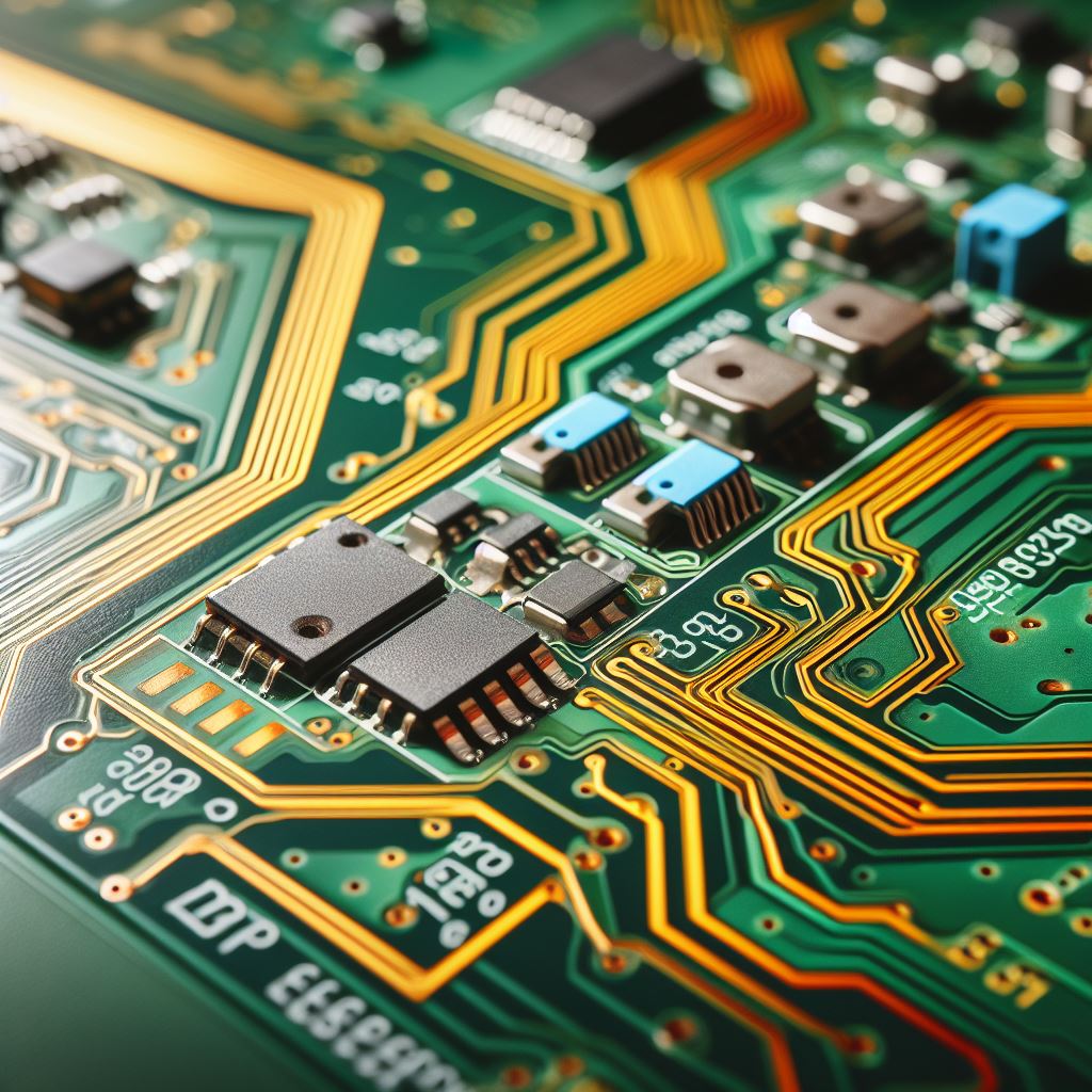
Grounding and power distribution are fundamental aspects of PCB design that play a crucial role in ensuring signal integrity, minimizing noise, and maintaining the overall functionality of the board. In this chapter, we will explore the principles of effective grounding and power plane design to create a stable and interference-free electrical environment.
7.1 Creating Effective Grounding Schemes
Single-Point Grounding: Establish a single, common ground point for all components and signals on the PCB. This helps prevent ground loops and ensures a consistent reference voltage.
Separate Analog and Digital Grounds: In mixed-signal PCBs, separate analog and digital ground planes can reduce interference between sensitive analog and noisy digital components.
Star Grounding: Use a star grounding topology, where all ground connections radiate from a single point. This minimizes the chances of ground loops and simplifies troubleshooting.
Ground Plane: Incorporate a dedicated ground plane on inner layers of the PCB to provide a low-impedance path for return currents and reduce electromagnetic interference (EMI).
7.2 Power Distribution
Power Planes: Similar to ground planes, use dedicated power planes to distribute power throughout the PCB. These planes provide a stable voltage reference and minimize voltage drops.
Decoupling Capacitors: Place decoupling capacitors near the power pins of ICs to reduce voltage fluctuations caused by transient currents. Choose the capacitance value based on the frequency of the noise you want to suppress.
Power Integrity: Ensure that power distribution traces and planes are designed to handle the expected current loads without voltage droops. Calculate trace widths and plane thicknesses accordingly.
Bypass Capacitors: Install bulk bypass capacitors at the input power source to filter out high-frequency noise from the power supply.
7.3 Minimizing Noise and Interference
Ground Plane Stitching: Use stitching vias to connect ground planes on different layers, especially when transitioning between ground planes with different reference potentials.
Signal Return Paths: Ensure that signal traces have a clear and low-impedance return path to the ground plane. Avoid routing signals over gaps in the ground plane.
Isolation: Isolate sensitive analog components or sections of the PCB from noisy digital sections to reduce the risk of interference.
Ferrite Beads: Integrate ferrite beads or inductors in power and signal lines to filter out high-frequency noise.
Shielding: For particularly sensitive components or RF applications, consider using shields or enclosures to block external electromagnetic interference.
7.4 Testing and Verification
Perform continuity and impedance tests on ground and power planes to ensure they are correctly connected and meet the desired impedance values.
7.5 Documentation
Document the grounding and power distribution scheme clearly in your design files. Include details about ground plane connections, decoupling capacitors, and power plane specifications.
Effective grounding and power distribution are essential for maintaining the integrity of your PCB's signals and minimizing noise and interference. By implementing proper grounding techniques, utilizing dedicated ground and power planes, and following best practices for power integrity, you can create a PCB design that operates reliably in various conditions.
Chapter 8: Signal Integrity and EMI/EMC
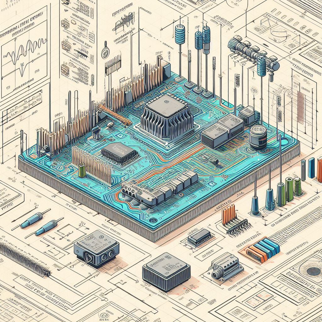
Signal integrity and electromagnetic compatibility (EMC) are paramount considerations in modern PCB design. Ensuring that your PCB operates with optimal signal quality and minimal electromagnetic interference (EMI) is essential for its functionality and compliance with regulatory standards. In this chapter, we will explore techniques for maintaining signal integrity and strategies to reduce EMI/EMC issues.
8.1 Maintaining Signal Integrity
Transmission Line Theory: Understand transmission line theory, which governs the behaviour of signals on traces. Ensure that traces carrying high-speed signals are impedance-matched to prevent signal reflections.
Termination: Properly terminate transmission lines to prevent signal reflections. Techniques like series termination resistors and parallel termination resistors can be employed.
Differential Signaling: Utilize differential signalling for high-speed data communication. This technique reduces susceptibility to common-mode noise and enhances noise immunity.
Signal Return Paths: Ensure clear and low-impedance return paths for signals. This may involve stitching vias or employing ground planes for reference.
Cross-Talk Mitigation: Minimize cross-talk between adjacent traces by maintaining appropriate spacing and using shielding techniques when necessary.
8.2 Strategies to Reduce EMI
Filtering: Incorporate filters, such as low-pass or common-mode chokes, to attenuate high-frequency noise on signal lines and power rails.
Shielding: For sensitive components or areas of the PCB, consider shielding techniques using conductive materials or enclosures to block electromagnetic radiation. XGR Technologies' Snapshot EMI shields represent a ground-breaking advancement in board-level shielding (BLS) solutions, effectively addressing and overcoming numerous challenges commonly encountered in the field of modern shielding technologies.
Grounding: Proper grounding practices, including single-point grounding and separating analog and digital grounds, can significantly reduce the emission of electromagnetic interference.
Component Placement: Thoughtful placement of components, especially high-frequency sources like oscillators or RF transceivers, can minimize their impact on other parts of the board.
PCB Layout: Follow best practices for PCB layout, such as reducing loop areas in signal paths, using solid ground planes, and avoiding abrupt changes in trace direction.
8.3 Compliance with EMC Standards
Regulatory Standards: Familiarize yourself with electromagnetic compatibility (EMC) standards applicable to your product's intended markets. These standards specify limits for emissions and immunity.
Pre-compliance Testing: Consider conducting pre-compliance testing to identify and address potential EMC issues before formal certification testing. This can save time and costs in the long run.
Simulation Tools: Utilize electromagnetic simulation software to model and analyse EMI/EMC behaviour in your design. These tools can help you make informed decisions during the design phase.
8.4 Design Validation
Testing: Perform signal integrity and EMI/EMC testing on prototypes or pre-production PCBs to verify their performance and compliance with standards.
8.5 Documentation
Document your signal integrity measures and EMI/EMC design strategies thoroughly in your design files. This documentation is essential for compliance testing and future design iterations.
Achieving robust signal integrity and addressing EMI/EMC concerns require careful consideration throughout the PCB design process. By implementing the techniques and strategies discussed in this chapter, you can develop a PCB that meets performance expectations and regulatory requirements.
Chapter 9: Thermal Management
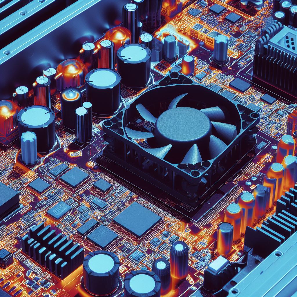
Effective thermal management is a critical aspect of PCB design, particularly as electronic components continue to shrink in size and increase in power density. Ensuring that your PCB can dissipate heat efficiently is essential for maintaining component reliability and performance. In this chapter, we will explore strategies for managing heat generation on the PCB and methods for effective cooling.
9.1 Heat Generation on the PCB
Identifying Heat Sources: Recognize components that generate significant heat, such as microprocessors, power amplifiers, or voltage regulators.
Power Dissipation: Calculate the power dissipation of these components based on their voltage and current ratings, and consider how this heat will affect nearby components.
Thermal Specifications: Refer to component datasheets for thermal specifications, including maximum operating temperatures and thermal resistance values.
9.2 Thermal Vias
Function: Thermal vias are copper-plated holes in the PCB that provide a path for heat to travel from the component to the inner or outer layers of the board.
Placement: Position thermal vias strategically beneath high-power components to enhance heat dissipation. Ensure that vias are adequately connected to power and ground planes for efficient conduction.
Via Arrays: Consider using arrays of thermal vias for larger components or those with multiple heat sources. This spreads heat more evenly across the board.
9.3 Heatsinks
Types: Select appropriate heatsinks based on your PCB's specific requirements. Options include passive heatsinks (finned metal), active heatsinks (with fans), and phase-change materials.
Component Attachment: Attach heatsinks securely to components with thermally conductive adhesive or mechanical fasteners. Ensure proper thermal contact between the component and heatsink.
Orientation: Orient heatsinks to maximize airflow and natural convection. In some cases, consider adding a fan for forced convection.
9.4 PCB Layout for Thermal Management
Component Spacing: Space heat-generating components to prevent localized heating. Avoid clustering them together, as this can lead to hotspots.
Heat Sinks for ICs: Some IC packages feature exposed pads on the underside, allowing direct attachment of a heatsink. Utilize these when applicable.
Power Plane Considerations: Ensure that power planes can act as effective heat spreaders. Use internal layers for heat dissipation if needed.
9.5 Simulations and Testing
Thermal Simulations: Use thermal simulation software to model and analyse heat distribution and dissipation in your PCB design. This helps identify potential hotspots.
Testing: Conduct thermal testing on prototypes or pre-production PCBs to validate your thermal management strategies and ensure they meet component specifications.
9.6 Documentation
Document your thermal management strategies, including the placement of thermal vias, heatsinks, and any thermal simulation results, in your design files. This documentation aids in design validation and future iterations.
Efficient thermal management is essential for preventing component overheating and ensuring the long-term reliability of your PCB. By implementing the techniques discussed in this chapter, you can effectively address heat generation and cooling concerns in your PCB design.
Chapter 10: Design for Manufacturability (DFM)
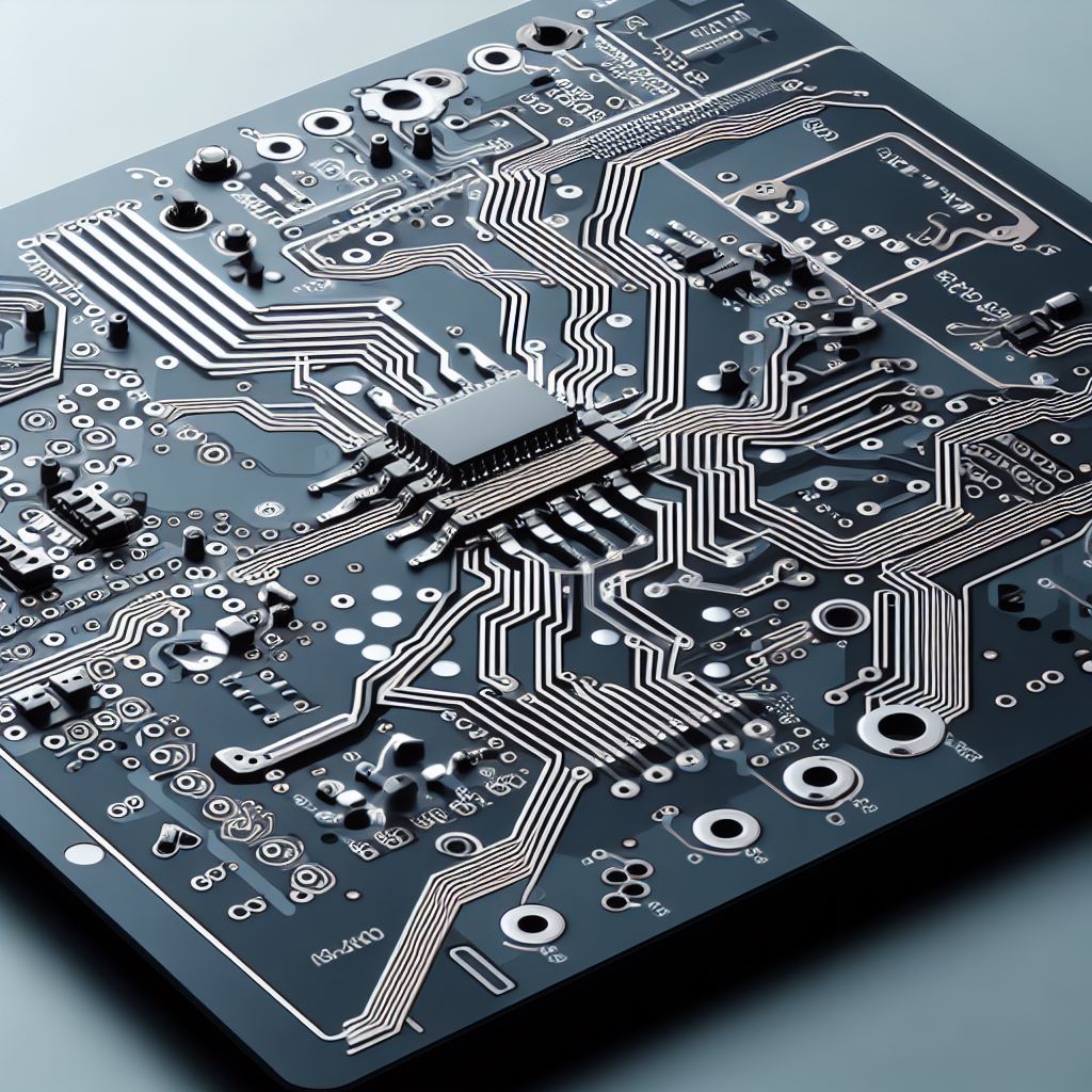
Design for Manufacturability (DFM) is a crucial aspect of PCB design that focuses on streamlining the manufacturing and assembly processes while minimizing costs. In this chapter, we will explore essential guidelines and considerations to simplify PCB fabrication and assembly, ensuring a smooth transition from design to production.
10.1 Guidelines to Simplify PCB Fabrication
Layer Count: Minimize the number of PCB layers wherever possible. Fewer layers reduce material costs and simplify the manufacturing process.
Standard Materials: Use standard PCB materials and thicknesses to avoid special orders that can add both time and expense to production.
Component Footprints: Utilize standardized component footprints whenever feasible. This ensures that components are readily available and reduces the need for custom manufacturing.
Clearance and Tolerances: Maintain adequate clearance between components and traces to prevent manufacturing errors and reduce the risk of shorts.
Hole Sizes: Design holes with standard sizes to simplify drilling and reduce production costs. Non-standard hole sizes may require custom tooling.
10.2 Design Considerations for Cost-Effective Production
Component Placement: Organize components logically to minimize trace lengths and reduce the complexity of routing. This can lead to shorter manufacturing times.
Silkscreen and Markings: Clearly label components, polarity, and reference designators on the silkscreen layer. This aids assembly technicians and reduces the likelihood of mistakes.
Through-Hole vs. Surface Mount: Consider using surface-mount components when possible, as they are typically easier and faster to assemble than through-hole components.
Test Points: Include test points on the PCB to facilitate functional testing and troubleshooting during production.
Panelization: For smaller PCBs, consider panelization, where multiple copies of the same board are arranged on a larger panel. This can improve production efficiency.
10.3 Prototyping and Validation
Before transitioning to mass production, create prototypes to verify the design's functionality and manufacturability.
Perform design rule checks (DRC) and manufacturing rule checks (MRC) to identify and rectify potential production issues.
10.4 Documentation and Collaboration
Provide comprehensive documentation, including Gerber files, assembly drawings, and a bill of materials (BOM), to the manufacturer to ensure accurate production.
Collaborate closely with your PCB manufacturer and assembly house. Early communication can help identify and address potential manufacturing challenges.
10.5 Design Iteration
Be prepared for design iterations based on feedback from the manufacturing and assembly processes. Continuously improve your designs to enhance manufacturability and reduce costs.
By adhering to these DFM guidelines and considering cost-effective production strategies, you can simplify the PCB manufacturing and assembly processes, reduce production costs, and ensure a smoother transition from design to production. This holistic approach to PCB design not only benefits your project's bottom line but also enhances its overall success.
Chapter 11: Design Validation and Simulation

Design validation through simulations is a critical step in the PCB design process. It allows you to assess and refine your design before physical prototypes are produced, reducing the risk of costly errors and ensuring optimal performance. In this chapter, we'll explore the importance of design validation and the use of various simulations, including SPICE, SI (Signal Integrity), and PI (Power Integrity), for thorough design verification.
11.1 The Importance of Design Validation
Risk Mitigation: Design validation helps identify and address potential issues early in the design process, reducing the risk of costly errors during production.
Performance Optimization: Simulations enable you to optimize your design for factors like signal integrity, power integrity, and thermal management.
Time and Cost Savings: Identifying and rectifying design issues through simulation is more cost-effective and time-efficient than making changes during later stages of production.
11.2 SPICE Simulations
Overview: SPICE (Simulation Program with Integrated Circuit Emphasis) is a powerful tool for analysing analog and digital circuits. It simulates circuit behaviour based on component models, helping you evaluate performance, stability, and functionality.
Applications: Use SPICE simulations to verify the functionality of analog components, such as amplifiers, filters, and oscillators. It's also valuable for assessing the transient behaviour of digital circuits.
11.3 Signal Integrity (SI) Simulations
Overview: SI simulations assess the quality of signal transmission in high-speed digital designs. They predict how signals will behave concerning factors like reflection, crosstalk, and timing.
Applications: SI simulations are vital for ensuring that high-speed data buses, such as DDR memory interfaces or PCIe connections, operate correctly without signal degradation or data corruption.
11.4 Power Integrity (PI) Simulations
Overview: PI simulations analyse how power is distributed on the PCB, helping identify voltage fluctuations, noise, and areas of excessive power dissipation.
Applications: PI simulations are crucial for guaranteeing stable power delivery to all components, reducing the risk of voltage droops that could impact functionality.
11.5 Thermal Simulations
Overview: Thermal simulations model heat dissipation and distribution on the PCB. They help assess the effectiveness of heatsinks, thermal vias, and other cooling solutions.
Applications: Thermal simulations are vital when working with high-power components or in environments where temperature regulation is critical.
11.6 Integration of Simulations
Combined Approach: Combining SPICE, SI, PI, and thermal simulations provides a comprehensive view of your design's performance, addressing electrical, thermal, and mechanical aspects.
Iteration: Use simulation results to iterate and refine your design, ensuring it meets all performance and reliability requirements.
11.7 Prototyping and Testing
Physical Validation: While simulations are invaluable, physical prototypes should still undergo testing to validate real-world performance and reliability.
Iterative Process: Continue to refine your design based on prototyping and testing results, closing the loop between simulation and physical validation.
Design validation through simulations is a cornerstone of modern PCB design. It empowers you to fine-tune your designs, optimize performance, and reduce the risk of issues arising during production. By leveraging tools like SPICE, SI, PI, and thermal simulations, you can ensure that your PCB meets or exceeds all requirements and specifications.
Chapter 12: Design for Testability (DFT)
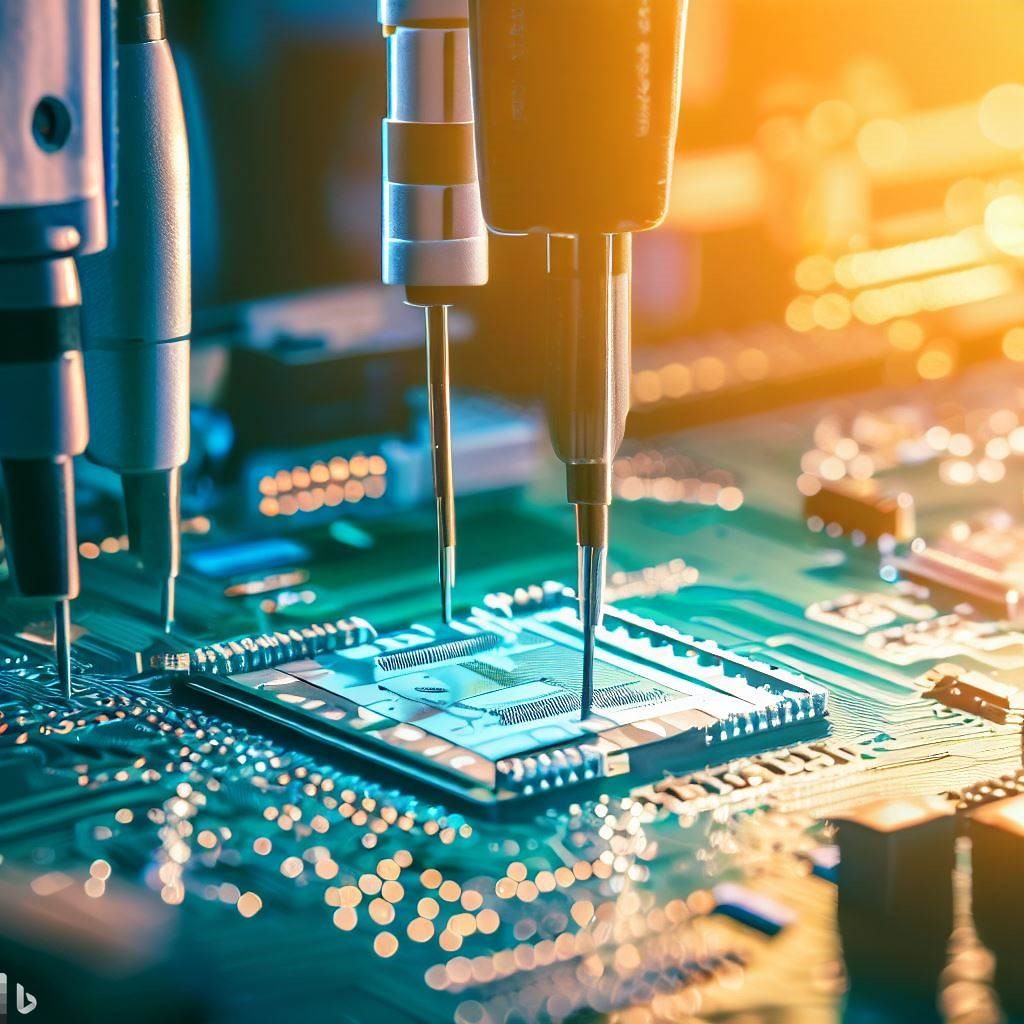
Design for Testability (DFT) is a fundamental consideration in PCB design. It involves incorporating features that facilitate efficient testing and debugging during both the manufacturing process and the product's lifecycle. In this chapter, we'll delve into the importance of DFT and explore strategies for implementing it effectively in your PCB designs.
12.1 The Significance of DFT
Early Issue Detection: DFT features enable early detection of manufacturing defects, ensuring that faulty boards are identified and rectified before reaching the end-user.
Reduced Debugging Time: Well-designed testability features simplify the debugging process, reducing the time and resources required for troubleshooting.
Enhanced Reliability: Effective DFT strategies contribute to improved product reliability by identifying and addressing potential issues promptly.
12.2 Key DFT Considerations
Test Points: Incorporate test points in your PCB design at strategic locations, allowing easy access for test probes during manufacturing and later servicing.
Boundary Scan (JTAG): Implement boundary scan architecture (Joint Test Action Group) to facilitate testing of complex digital circuits, enabling comprehensive coverage.
Access to Critical Nodes: Ensure that crucial nodes, such as power rails and critical signals, are accessible for testing and monitoring.
Built-In Self-Test (BIST): Consider integrating BIST capabilities into your design, enabling the board to test itself for faults during power-up or specific operational states.
12.3 Designing for Manufacturing Test
Design Rules for DFT: Collaborate closely with your PCB manufacturer to establish design rules that align with DFT requirements, ensuring seamless testing during production.
Automated Test Equipment (ATE): Design your PCB to be compatible with automated test equipment, allowing efficient, high-throughput testing.
Functional Testing: Define test points and procedures for functional testing to verify that the assembled PCB meets all performance requirements.
12.4 Debugging and In-Circuit Testing
In-Circuit Test (ICT): Leverage ICT fixtures and procedures to identify manufacturing defects, including short circuits and open connections.
Boundary Scan Testing: Utilize boundary scan testing to assess digital components, ensuring proper operation and connectivity.
12.5 Documentation and Collaboration
Detailed Documentation: Provide comprehensive documentation that includes test point locations, boundary scan information, and BIST instructions to assist manufacturers and technicians.
Collaboration with Test Engineers: Work closely with test engineers to ensure that your DFT features align with their testing strategies and equipment.
12.6 Prototyping and Verification
Prototyping: Validate your DFT features during the prototyping phase to verify their effectiveness in identifying and addressing manufacturing defects.
Iterative Improvement: Continuously refine your DFT strategies based on feedback from testing and manufacturing to enhance their efficiency.
12.7 Product Lifecycle Considerations
Accessibility for Servicing: Ensure that DFT features remain accessible during the product's lifecycle, allowing for efficient servicing and debugging in the field.
Firmware Upgrades: Design your PCB to support firmware upgrades, enabling ongoing improvements and bug fixes.
Design for Testability is a proactive approach that enhances the reliability and efficiency of PCB manufacturing and servicing processes. By implementing DFT features and collaborating closely with manufacturing and testing experts, you can streamline production, reduce costs, and ensure that your PCBs meet the highest quality standards.
Chapter 13: Documentation and Collaboration

Effective documentation and collaboration are paramount in successful PCB design projects. This chapter delves into the importance of creating comprehensive design documentation and explores collaborative tools and practices that enable PCB design teams to work seamlessly and efficiently.
13.1 Comprehensive Design Documentation
Schematic Diagrams: Develop clear and detailed schematic diagrams that depict the circuit's architecture, components, and connections. Include reference designators, values, and critical notes.
Bill of Materials (BOM): Maintain an up-to-date BOM that lists all components, their specifications, suppliers, and part numbers. This document is essential for procurement and assembly.
Gerber Files: Generate accurate Gerber files that communicate the PCB's layout, layer stackup, and manufacturing details to fabricators.
Assembly Drawings: Create assembly drawings that guide technicians in placing components correctly during PCB assembly.
Fabrication Drawings: Provide detailed fabrication drawings to communicate design intent to manufacturers, including dimensions, tolerances, and material specifications.
Design Guidelines: Document design guidelines and constraints to maintain consistency across your team's projects.
13.2 Collaborative Tools
PCB Design Software: Utilize PCB design software that supports collaboration features, allowing multiple team members to work on the same design concurrently.
Version Control Systems: Implement version control systems like Git to track design changes, manage revisions, and facilitate collaboration among team members.
Collaboration Platforms: Leverage collaboration platforms such as Slack, Microsoft Teams, or project management tools like Trello or Asana to facilitate communication and file sharing among team members.
Cloud-Based Storage: Use cloud-based storage solutions like Dropbox or Google Drive to store and share design files securely.
13.3 Collaborative Practices
Regular Meetings: Schedule regular team meetings to discuss progress, challenges, and design decisions. Video conferencing can enhance remote collaboration.
Design Reviews: Conduct design reviews where team members scrutinize the design, identify potential issues, and propose improvements.
Clear Communication: Maintain open and clear communication channels to ensure that everyone is aligned on project objectives and timelines.
Documentation Standards: Establish consistent documentation standards and naming conventions to streamline information retrieval and maintain organization.
13.4 Documenting Design Changes
Change Logs: Maintain change logs to record design modifications, reasons for changes, and the individuals responsible for implementing them.
Revision Control: Implement revision control practices to ensure that design files are consistently labeled with version numbers and dates.
13.5 Collaboration Across Teams
Interdisciplinary Collaboration: Encourage collaboration between PCB design teams and other departments, such as mechanical engineering, to address cross-disciplinary challenges.
Supplier Collaboration: Foster collaboration with component suppliers and manufacturers to ensure that design and procurement align seamlessly.
13.6 Prototyping and Testing Documentation
Prototyping Logs: Document the prototyping process, including test results, observations, and any modifications made to the design.
Testing Procedures: Maintain detailed testing procedures and results to validate the PCB's performance and compliance with specifications.
Effective documentation and collaboration practices are the cornerstones of successful PCB design projects. By creating comprehensive design documentation and leveraging collaborative tools and practices, PCB design teams can streamline their workflows, enhance communication, and ultimately deliver high-quality PCBs that meet or exceed all requirements
Chapter 14: Regulatory Compliance
Regulatory compliance is a critical aspect of PCB design, especially when your PCB will be used in specific industries or applications. In this chapter, we will explore the importance of ensuring that your design meets industry-specific standards and regulations. We'll also discuss strategies for navigating the certification process.
14.1 Industry-Specific Standards
Understanding Standards: Familiarize yourself with industry-specific standards that apply to your PCB design. These standards may include safety, electromagnetic compatibility (EMC), and environmental regulations.
Examples of Standards: Depending on your application, you may need to adhere to standards such as UL 60950 (safety of information technology equipment), IPC-A-610 (acceptability of electronic assemblies), or ISO 9001 (quality management systems).
14.2 Compliance Assessment
Early Assessment: Begin assessing compliance requirements early in the design process to identify potential issues and make necessary adjustments.
Testing and Verification: Conduct testing and verification procedures to ensure that your PCB design complies with relevant standards. This may involve environmental testing, EMC testing, or safety assessments.
14.3 Certification Process
Choosing Certification Bodies: Select reputable certification bodies or agencies that are recognized in your industry. They will guide you through the certification process.
Documentation: Prepare comprehensive documentation that demonstrates your design's compliance with standards. This may include test reports, design files, and compliance statements.
Testing and Evaluation: Submit your design for testing and evaluation by the certification body. Be prepared to address any issues or concerns that arise during this process.
14.4 Compliance in Design
Design Considerations: Integrate compliance considerations into your PCB design from the outset. This includes selecting components that meet relevant standards and designing for EMC and safety.
Prototyping for Compliance: Prototyping is an opportunity to verify that your design meets compliance requirements before moving to mass production.
14.5 Environmental Regulations
RoHS and REACH: Understand and comply with environmental regulations like the Restriction of Hazardous Substances (RoHS) and Registration, Evaluation, Authorisation and Restriction of Chemicals (REACH) directives if applicable.
14.6 Navigating Challenges
Iterative Process: Navigating compliance can be challenging, and it often involves an iterative process of design adjustments and retesting.
Expert Consultation: Seek guidance from experts or consultants who specialize in regulatory compliance for your industry.
14.7 Record Keeping
Maintaining Records: Keep meticulous records of your compliance efforts, including design changes, testing results, and correspondence with certification bodies.
14.8 Continuous Compliance
Updates and Re-Certification: Be aware that standards and regulations may change over time. Plan for updates and re-certification to ensure continued compliance throughout the product's lifecycle.
Ensuring regulatory compliance is essential to both the safety and marketability of your PCB design. By understanding and adhering to industry-specific standards, navigating the certification process effectively, and maintaining rigorous record-keeping practices, you can confidently deliver PCBs that meet regulatory requirements and stand up to scrutiny.
Chapter 15: PCB Prototyping and Iteration

Prototyping and iteration are integral parts of the PCB design process. In this chapter, we will explore best practices for creating PCB prototypes and discuss the crucial role of iteration and refinement in PCB design.
15.1 Prototyping Basics
Why Prototype: Prototyping allows you to validate your design concept, test functionality, and identify potential issues before mass production.
Prototyping Methods: Choose from various prototyping methods, including bread boarding, per boarding, and PCB fabrication. Each has its advantages based on your project's complexity.
Proof of Concept: Use the prototype as a proof of concept to verify that your design can achieve its intended purpose.
15.2 PCB Prototyping Best Practices
Component Selection: Use production-grade components in your prototype to ensure accurate testing and performance evaluation.
Layout and Wiring: Follow proper layout and wiring practices even in prototypes to minimize signal interference and ensure realistic testing conditions.
Testing Strategy: Plan a comprehensive testing strategy for your prototype, including functionality, performance, and environmental testing.
Documentation: Maintain thorough documentation for your prototype, including schematic diagrams, component lists, and design notes.
15.3 Iteration and Refinement
The Iterative Process: Expect that your initial prototype may not be perfect. Iteration involves a cycle of testing, identifying issues, making design changes, and building new prototypes.
Continuous Improvement: Embrace the iterative process as an opportunity for continuous improvement. Each iteration brings you closer to a refined and optimized design.
Addressing Issues: Pay close attention to issues identified during testing. These may include functional problems, signal integrity issues, or thermal challenges.
15.4 Advanced Prototyping Techniques
Rapid Prototyping: Explore rapid prototyping methods like 3D printing for enclosures or flexible PCB fabrication for specialized applications.
Firmware and Software Prototyping: In addition to hardware, prototype your firmware and software to ensure seamless integration with your PCB design.
15.5 The Role of Simulation
SPICE Simulation: Use SPICE (Simulation Program with Integrated Circuit Emphasis) to model and simulate circuit behaviour before building a physical prototype.
Signal Integrity Simulation: Employ signal integrity simulations to analyse and optimize high-speed signal paths on your PCB.
15.6 Collaborative Prototyping
Team Collaboration: Involve team members from various disciplines, including hardware, software, and mechanical engineering, in the prototyping and testing process.
External Feedback: Seek external feedback from peers, mentors, or industry experts to gain fresh perspectives on your design.
15.7 Balancing Time and Resources
Efficiency: Balance the depth of your prototyping efforts with project timelines and available resources. Early prototypes may focus on high-level functionality, while later iterations dive deeper into performance optimization.
15.8 Final Prototyping Phase
Pre-Production Prototypes: Before moving to mass production, build pre-production prototypes that closely resemble the final product. These prototypes serve as a final validation step.
15.9 Documentation and Handoff
Documenting Changes: Document all design changes made during the prototyping and iteration phases. This documentation will be invaluable for future reference and when handing off the design for production.
Prototyping and iteration are essential phases in PCB design. By following best practices for creating prototypes, embracing the iterative process, and leveraging advanced techniques like simulation, you can refine your design, resolve issues, and ensure that your PCB meets or exceeds its intended specifications.
Conclusion: Mastering PCB Design
In our comprehensive guide to PCB design, we've embarked on a journey through the intricate world of printed circuit boards. We've explored the fundamental principles, intricate techniques, and critical considerations that define the art and science of PCB design. As we conclude our journey, let's summarize the key takeaways from this extensive guide and reflect on PCB design as both an art and a science.
Key Takeaways:
- Fundamentals First: PCB design begins with understanding the basics. Familiarize yourself with components, schematics, and circuit theory. A strong foundation is essential.
- Design Software: Choose the right PCB design software for your project. Each tool has its strengths, so select one that aligns with your needs and skill level.
- Component Selection: Components are the building blocks of your design. Pay meticulous attention to their specifications, compatibility, and availability.
- Layer Stackup: Layer stackup decisions impact signal integrity, power distribution, and thermal management. Tailor your stackup to your project's requirements.
- Routing and Traces: Proper routing techniques ensure signal integrity and minimize interference. Maintain appropriate trace widths, spacing, and controlled impedance.
- Grounding and Power Planes: Effective grounding and power distribution are crucial for noise reduction and stable voltage supply.
- Signal Integrity and EMI/EMC: Maintain signal integrity by controlling impedance and minimizing reflections. Implement EMI/EMC strategies to meet compliance requirements.
- Thermal Management: Overheating can be detrimental. Use thermal vias, heatsinks, and other techniques to manage heat effectively.
- Design Validation: Simulation tools like SPICE, SI, and PI simulations aid in verifying your design's functionality and performance.
- Documentation: Thorough documentation ensures a clear and organized design process. It simplifies collaboration and troubleshooting.
- Regulatory Compliance: Ensure your design complies with industry-specific standards and regulations. Early assessment and testing are critical.
- Prototyping and Iteration: Prototyping allows you to validate your design and identify issues before mass production. Embrace iteration as a path to refinement.
- Collaboration: Collaboration among multidisciplinary teams and seeking external feedback can lead to innovative and optimized designs.
- Efficiency: Balance prototyping depth with project timelines and resources. Early prototypes validate concepts, while later iterations optimize performance.
- Simulation and Advanced Techniques: Leverage advanced techniques like SPICE simulations, signal integrity analysis, and rapid prototyping to enhance your design process.
The Art and Science of PCB Design:
PCB design is both an art and a science. It blends technical precision with creative problem-solving. A successful PCB designer not only understands the intricacies of electrical circuits but also possesses the ability to envision how components interact in the real world. It's a discipline that demands attention to detail, a passion for innovation, and a dedication to continuous learning.
In closing, mastering PCB design is an ongoing journey. With each project, you'll refine your skills, adapt to new technologies, and tackle fresh challenges. Remember that the best designs often emerge from the intersection of knowledge, experience, and the relentless pursuit of perfection. So, embrace PCB design as the art and science that it is, and let your creations pave the way for technological innovation.


